R&D [Research and Development Area]
Electronic Materials
In harnessing our extensive understanding of photopolymers, material science and coating technologies acquired through the development and manufacture of printing and plate-making materials, we have formulated uniquely characteristic photoresist films for use in photofabrication processes in electronics and other fields.
High Resolution Technology
Display devices and mobile information terminals are becoming increasingly sophisticated. The high density of substrate wiring and components is resembling the complexity of semiconductor devices in their infancy, and even the processing precision required for peripheral components is approaching the realm of microfabrication where liquid photoresists were once primarily used. We are utilizing our precision coating technology to develop high-resolution dry film resists that can be handled in a simple process in response to this trend toward high-density mounting.
Examples of processing using our products
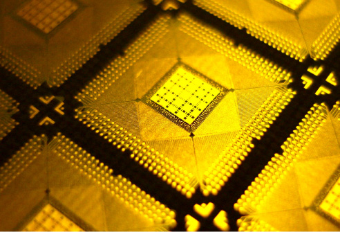
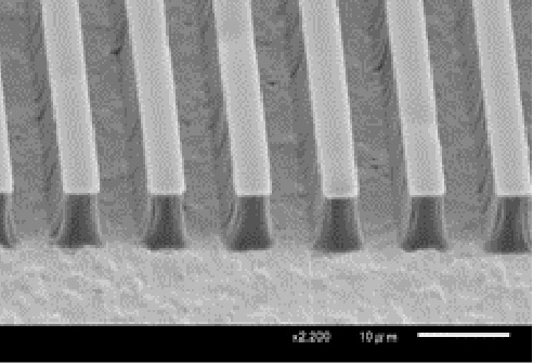
Line/Space=5/5µm
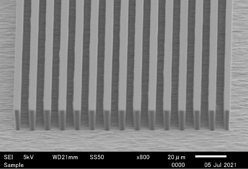
Line/Space=5/5µm
High Performance and Durability Technology
In recent years, the use of difficult-to-process materials has become common in the electronics field, such as ceramic heat-dissipating substrates for LED surface mounting, thick copper substrates for power devices, titanium plates for fuel cell separators, and thin glass substrates for display devices. These materials require precise processing using photo fabrication. To meet these special processing requirements, we are developing technologies to expand the possibilities and scope of various processing methodologies, such as photoresists with film strength that can withstand physical grinding (sandblasting) and photoresists with high chemical resistance that can withstand high-intensity etching processes.
Examples of processing using our products
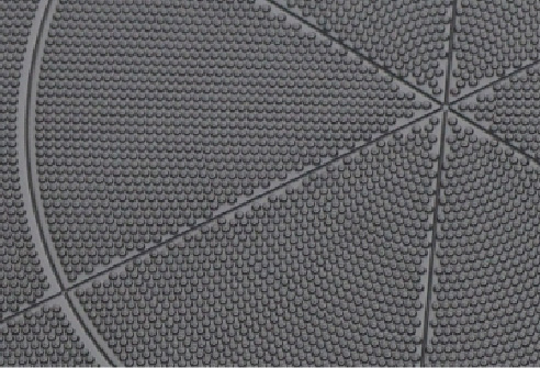
Electrostatic Chucks : Semiconductor Manufacturing Jigs
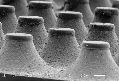
Glass substrate Grinding 700µm
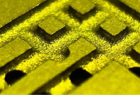
Titanium plate channel, groove depth 400µm
